In Part 1 of this series, I went over the historical background of CSYNC, including its purpose and how it is intended to be generated and then subsequently used for conveying television timing information. Within that description, I highlighted some key properties of the 480i CSYNC waveform and how that translates over to creating various 240p “flavors”. Since the advent of TV, personal computing and other applications have borrowed ideas from the engineering principles initially set forth in the complex design of television’s CSYNC structure. Along the way, a few of these principles have been ignored or overlooked to justify simpler solutions. Therefore, there are extremely common implementations from those early PCs days which have propagated throughout the decades and are thought to be “standardized” or “correct”. In this Part 2, I will cover the two most commonly used methods to form a CSYNC output from existing HSYNC and VSYNC signals, and why they can cause issues with equipment trying to use this resultant signal. Unless noted otherwise, we will be mainly working with the “Cookies & Cream” flavor of 240p (see Part 1) when discussing the sync waveforms.
AND Logic
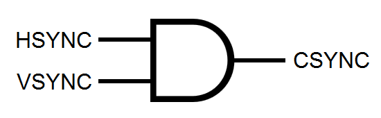
There are tons of various flavors of this type of method, and they might not necessarily show up as an AND logic gate symbol (like the one shown above) in a schematic. For example, it could be an OR gate with input polarities flipped or a set of discrete components (diodes, resistors, transistors, etc.) implementing the logic in some approximated way. However, the fundamental principle is the same. The idea here is for CSYNC to normally push out the HSYNC information, but when VSYNC becomes active it completely overrides the HSYNC. An example of the ideal input/output waveforms passing through this type of logic is shown below.
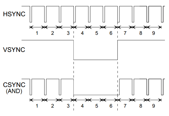
If this CSYNC waveform looks familiar, it’s because it’s very similar to the first step (Step A) in deriving the correct 480i CSYNC as described in Part 1. It makes sense because this is the first logical step in trying to combine the two types of syncing information into one signal. Therefore the problem that this naive implementation causes is the same as was described in Part 1: the HSYNC information is lost during VSYNC and the display device will lose horizontal lock…..unless it has a mechanism which expects this scenario and can avoid it or correct for it. The 2nd part of the previous statement is key here and provides a justification for this method to be used in the first place. Many direct analog systems found in older computer CRTs are simply more tolerant, by their very operational nature, to missing a few HSYNC pulses while the electron gun is off-screen. They’ll lose sync briefly while off-screen and either recover completely before active video starts again or take slightly longer causing only minor distortion/tearing at the top of the screen. However. more modern systems are based on something called a digital phase-locked-loop (or PLL for short), which can cause much more severe problems for the end-user when used with a wonky CSYNC input.
An extremely rough description of a PLL would be a device that generates an internal signal, locks onto an external reference signal, and compares the two to create a new version of that internal signal that’s in phase relationship with the external reference. In a typical modern system, the PLL operates on HSYNC (sometimes called LLPLL for “line-locked” PLL) and assumes this incoming signal is consistent up to a certain point. This certain point would be the PLL’s “lock-in range” or “hold-in range” [NOTE: these ranges are somewhat different, but assume for now they are the same]. When designing a PLL, the engineers have to set this window and there are trade-offs involved. If they set the lock/hold range too wide, then the PLL can take too long to lock and/or the output signal can drift around very easily resulting in an unstable system. Set it too narrow, and the PLL will lose lock easily for input signals with even the slightest of flaws. If you’ve ever experienced a modern flat screen HDTV display a black screen or have its picture flashing on/off quickly, then you are witnessing its PLL rapidly switching from locked to unlocked status. This is because a modern video system will completely disable its video output when the PLL is reporting that it is not in its locked state. Many video decoder (video ADC) chips have a feature called “coast” which can tell the PLL to ignore the reference input signal for a certain amount of time and continue to output its own internally generated HSYNC during that time. If this coast time is short enough, then the internally generated HSYNC won’t drift off too much before the coast period is over, when it would then re-lock onto the reference and begin correcting itself again. Coasting is commonly used in well-designed video PLLs to solve the problem of bad or out-of-spec CSYNC inputs. In the specific case of dealing with a CSYNC created from AND logic, the PLL will generate its own HSYNC pulses during the VSYNC portion to completely eliminate the missing pulses problem, unbeknownst to the user.
If you notice I did not mention interlacing here, where the HSYNC pulses near and around VSYNC are extremely vital in making an interlaced system work. Therefore this type of psuedo-CSYNC creation method is more suited for progressive video, which is why you find it used in older computing and arcade systems. For example, here is an oscilloscope plot from a Sega Master System (Model 1) which shows that this version of the SMS video processor (VDP) implements the CSYNC via AND logic before spitting it out to the world. [NOTE: there is a slight glitch at the beginning of the VSYNC portion, which will be addressed later in this article.]
![[Top] CSYNC from a Sega Master System (Model 1)[Bottom] Zoomed-in version of the top](/s/sms_and.png)
[Top] CSYNC from a Sega Master System (Model 1)
[Bottom] Zoomed-in version of the top
XNOR Logic

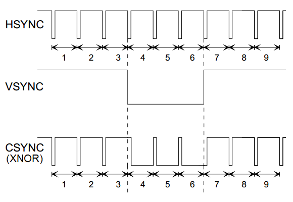
The most commonly used method for generating CSYNC is via XNOR (inverted-exclusive-OR) logic. Again, you might find this implemented slightly differently, such as an XOR gate (XNOR without the inverting part) along with swapped input polarities on one or both of the incoming HSYNC and VSYNC signals. Anyway, this method attempts to resolve the “dead period” of having no HSYNC pulses during the VSYNC portion as found when using AND logic. An example of the ideal input/output waveforms passing through this type of logic is shown below.
The problems associated with an XNOR-generated CSYNC are not as obvious as with the AND logic case. At a quick glance, it looks fine, so a more in-depth look is required while comparing it to a correctly generated CSYNC.
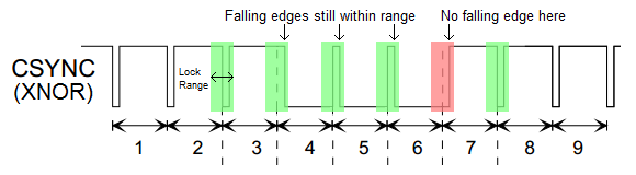
The main problem is that although there are pulses now in the VSYNC region, they are not in the correct position. A proper CSYNC has all its falling edges line up with the original HSYNC falling edges, and here they do not. Put another way, this violates the property established in Part 1 of requiring a consistent length of time between each falling edge throughout the entire CSYNC waveform. This can wreck havoc on the receiving device since there’s no way to tell a video system: “Hey, switch between using falling edges to rising edges just in this one window…..ummm but only when you get an XNOR generated CSYNC….how do you detect that??? I dunno, good luck!….oh and also figure out how to handle the missing edge at the beginning of that window.”
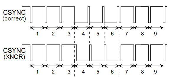
Just as before, we can consider the practical impact of such an error in the signal. Many CRT systems will be highly tolerant or immune to this just as in the AND logic case. Considering a modern system which relies on a PLL, this can cause the same or similar problems as in the AND case. A PLL with a well thought-out coast system will be able to ignore the incorrect pulses and regenerate its own. Fortunately, it can still be less of an issue compared to AND logic because even a PLL with no coasting ability might still be able to remain locked during the brief VSYNC section. This can happen if the PLL’s lock/hold range is set wide enough to still catch most of the falling edges of the misaligned pulses. An example of this possibility is shown below.
Therefore, XNOR logic is definitely a step above AND logic in nearly every imaginable scenario. However, there is an additional precaution to take when implementing an XNOR based system, which you don’t have to consider in the typical AND case. This is the property of an XNOR gate to generate glitches when both signals change state at the same time or very close to the same time. For example, when VSYNC transitions low the HSYNC also transitions low. It’s impossible for the transitions of both signals to happen at the exact same time, so depending on the properties of the device handling the logic and all the circuitry/wires leading up to that device you are likely to generate an extra very short pulse near those transitions. An example of this is shown below, taken from a Sega Genesis running in Master System mode which uses XNOR logic for its VDP’s legacy mode to generate and output the CSYNC signal. [NOTE: this signal does not match up exactly with the drawings above and this discrepancy will be covered a bit later in this article.]
![[Top] CSYNC from a Sega Genesis running in Master System mode[Bottom] Zoomed-in version of the top](/s/genesis_xnor.png)
[Top] CSYNC from a Sega Genesis running in Master System mode
[Bottom] Zoomed-in version of the top
If the glitch at the beginning of VSYNC is long enough it could be seen as an extra falling edge and throw the receiving system off. One way to combat this is to filter out any possible transition glitches by following the XNOR gate with an RC circuit driving into a Schmitt trigger digital logic buffer as shown below. The idea here is to select RC values which would snuff out glitches under a certain maximum width for your particular XNOR implementation. Keep in mind there is a trade-off here since this method can skew the widths of the pulses you want to keep, so it’s only good for very short glitches.
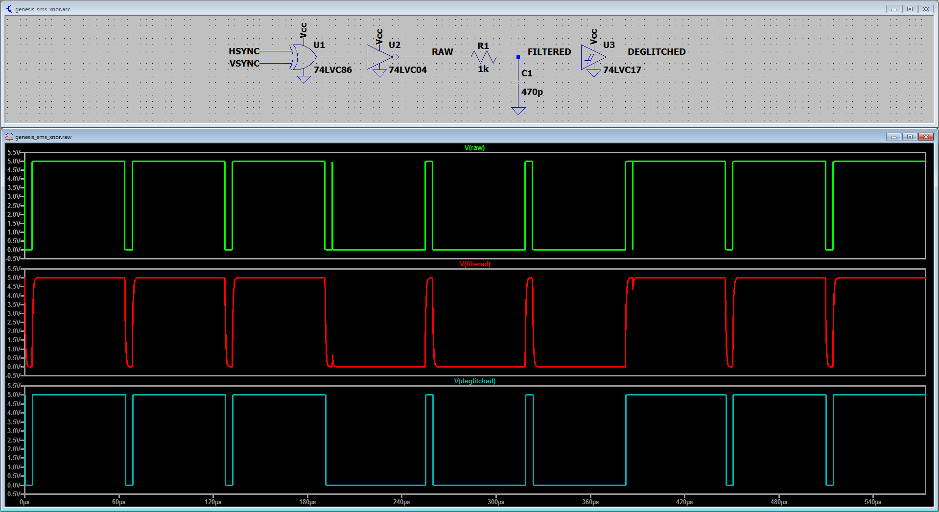
A circuit simulation of the proposed deglitch filter for Sega Genesis’s legacy XNOR output. Components values were selected to suppress glitches of roughly 100ns or less in length.
Return to Your Positions
Much of the discussion above has an underlying assumption which needs to be addressed: the input HSYNC and VSYNC signals are ideal with proper positioning and widths. The first clue to this assumption not holding in practice is found in the Sega Master System oscilloscope plot in the first section where there is a glitch at the beginning of the VSYNC portion. This is caused by the Master System VDP using a VSYNC which is shifted by one HSYNC pulse-width to the right, before going into the AND gate. Because HSYNC is rising while VSYNC is falling in that region, there is a small period of time where both signals are high, causing the glitch. This glitch, if short enough, can be removed similar to how the XNOR glitches discussed above are removed. The Genesis running in Master System mode also uses the same shifted VSYNC for its XNOR operation and is the reason its oscilloscope plot doesn’t match the ideal waveforms either. Keep in mind that even if a non-shifted VSYNC was used, it wouldn’t change the fact that transition glitches are generated since this phenomena is inherent to using XNOR logic when two signals are simultaneously changing state. Only the position of the glitches would change.
There are more severe cases where the input signal structure is not close enough to ideal to be somewhat usable after combined together using simple logic gates. The most common real-life example I can think of is with the TurboGrafx-16 (or PC Engine). The expansion port has the raw HSYNC and VSYNC available as pins on this connector. The first problem is that the HSYNC pulse is way too wide for the format it’s trying to represent (240p/480i), almost by a factor of 2.5x. The second is how the VSYNC alignment is off by a few microseconds, which when using either AND logic or XNOR logic for generation results in glitches that are much too wide to be removed. In fact, a naive implementation of CSYNC using XNOR logic on these two input signals is what caused many compatibility issues with the first revisions of the Super SD System 3 (SSDS3) from TerraOnion. Subsequent revisions used the already combined CSYNC available from the expansion connector which, although not 100% correct, is much more reliable.
![[Left-half] HSYNC (blue) & VSYNC (yellow) on the TurboGrafx-16 expansion port along with a direct XNOR combination of them (violet).[Right-half] Internally generated CSYNC (violet) from the TurboGrafx-16’s video processor along with the same exp…](/s/tg16_csync.png)
[Left-half] HSYNC (blue) & VSYNC (yellow) on the TurboGrafx-16 expansion port along with a direct XNOR combination of them (violet).
[Right-half] Internally generated CSYNC (violet) from the TurboGrafx-16’s video processor along with the same expansion port HSYNC (blue) & VSYNC (yellow) for comparison. Notice the smaller pulse widths and the lack of glitches. This looks to be created from a completely different set of HSYNC & VSYNC found only within the video processor, which were XNOR-ed together and then deglitched.
If it’s in a datasheet, it’s GOTTA be true!
Having laid out most of the issues with them, why are methods such as AND or XNOR so common? I mean, nearly all the information you find on the internet points to either one of these two logic systems being THE WAY to perform this task. You even have block diagrams from well-known IC manufacturers mentioning XNOR for their internal CSYNC creation.
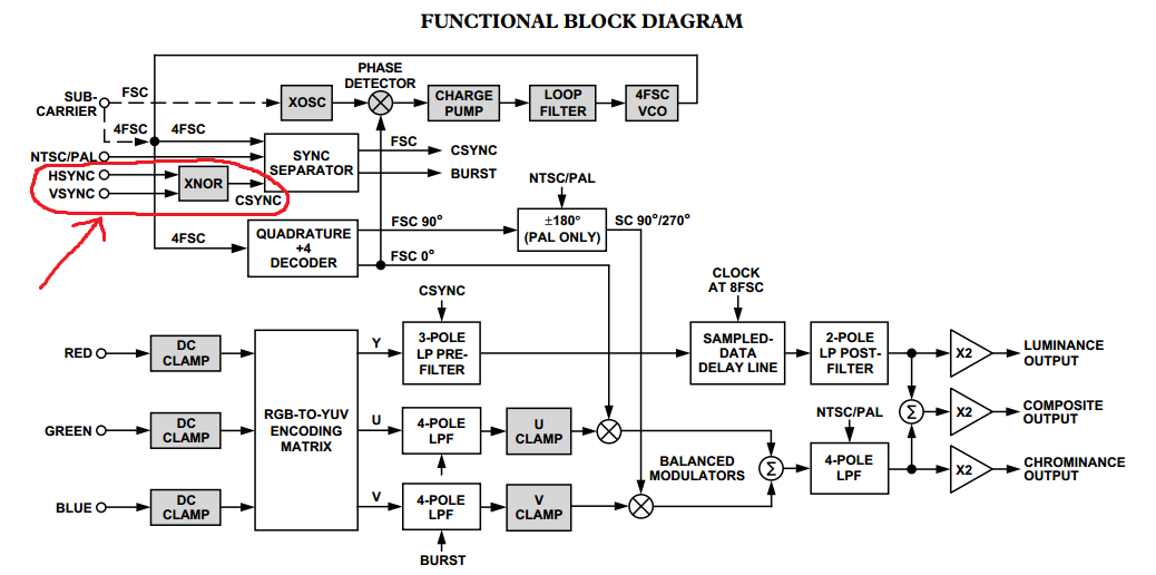
Snip from the AD724 Video Encoder datasheet from Analog Devices showing XNOR logic for CSYNC creation. This is misleading since, if you read further into the datasheet, the XNOR block shown here is only a small portion of the decoding logic used to generate the correct CSYNC patterns within the final Composite Video and S-Video outputs.
Although I think much of it is due to ignorance and an unwillingness to fully understand the nuances of analog video, I have to concede that the main reason these methods are still used is due to how they have the ability to work with several various input formats. So in a device which can accept many different HSYNC/VSYNC input formats, using something like an AND gate would be a very cost-effective way to have it “mostly” work across a wide range of inputs. This is especially true in the XNOR case and if you consider the VESA Display Monitor Timings (DMT) used for systems with VGA connectors. There are various VESA formats which deviate from the typical active-low sync practice, and can either have one or both of HSYNC/VSYNC be active-high instead. The XNOR method can produce some kind of a CSYNC output in all four of the possible polarity cases for HSYNC/VSYNC.
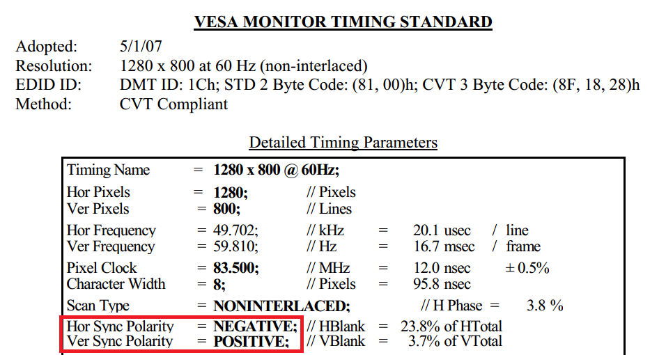
Snip from the VESA DMT document showing the differing sync polarities for 1280x800 @ 60Hz
The Cost of Doing Good Business
There are methods which attempt to correct CSYNC after it is generated from either AND or XNOR logic. TB476 is an Application Note from Renesas Electronics which details a system for doing this using ICs they manufacture. The final circuit is very large and complex, and it can’t universally correct for every type of format, especially any type of interlaced content. It’s still worth a read, since it’s one of the rare resources found on the internet that actually acknowledges and corroborates that these AND/XNOR based CSYNC generators cause problems.
For systems/devices that are only expecting and targeting one type of video format, I believe it’s worth implementing the extra time, resources, and effort to make sure the end-user has a trouble-free experience by generating a proper CSYNC signal. It’s not worth the risk relying on auxiliary safetynets, such as PLL coasting or wide lock/hold ranges, that may or may not be engineered into a receiving device. Even in multi-format systems which are already generating the HSYNC and VSYNC in the first place, you should be able to additionally generate a correct CSYNC with minimal extra effort and cost instead of opting for an AND/XNOR gate. This is especially true if you have to deal with realigning pulses prior to the logic gate and then filtering out glitches on the output, which is already a bunch of additional work in the first place. Lastly, it’s worth iterating once again that none of the methods discussed in this article can handle interlaced formats in a manner that even begins to approach a reasonable level of reliability.
Summary
The main takeaways from Part 2 are as follows:
1.) AND logic is the most basic form of CSYNC generation, and it was used commonly in early progressive-based video systems.
2.) XNOR logic is a step above AND logic in terms of reliability, as long as you mitigate the creation of transition glitches.
3.) For either of these methods to work reasonably well in enough scenarios, proper widths and positional alignment are required on the input HSYNC and VSYNC signals.
4.) These two simple logic gate methods have a unique benefit where they can be used effectively in a universal system dealing with many possible input formats.
5.) Fixing CSYNC errors after generation is very costly, unreliable, and non-universal. It’s also very difficult to do for interlaced systems.
In the upcoming Part 3 of this series, I’ll try to finally tackle proper CSYNC generation. If you are familiar with digital logic, both of the methods discussed above are types of “combinational logic”. The 2nd type of logic used in digital systems is known as “sequential logic”, and it’s what we need to use to engineer a correct CSYNC output.